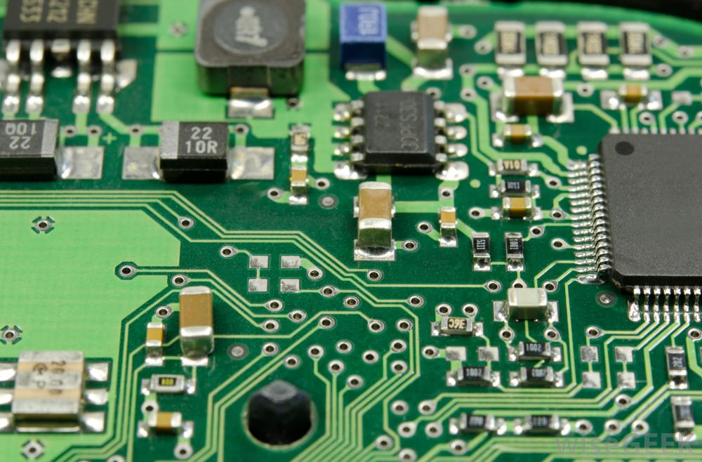
 PCB or Printed Circuit Boards are an important and irreplaceable part of every electronics since many years. Through this time the electronic devices are getting smaller and smaller in size and so are the board to board connectors as well as the PCB’s in them.
Usually when a PCB design is created a few things are to be taken care of like low power circuit boards, ensuring they are bug free, ensuring its functionality etc. There are guidelines and rules which need to be adhered to but in some extreme cases these guidelines are bendable to a certain extent depending on the demand of the design for e.g. spacing of the components in a dense design etc. Other rules like the electrical ones are to be followed strictly which if not done can cause serious damage.
Having said that some of the guidelines or rules are plain myths which might have been taught in school or a mentor that have been being followed blindly all through the years and which are believed to be real and unchangeable. When these myths are followed blindly without knowing they are the worth following or not it can spell trouble for the PCB designs which makes it very important to know what these common myths are.
So let us have a look at these myths that are guaranteed to blow your mind:
1. Electric schematic is the only tough work involved and the rest is easy:
Electric schematic is just a part of the whole process. Although it is a simple two step process wherein the required components are placed and the wires and traces are connected to the appropriate points. But that is not all. There are many more factors that are to be bought under consideration like:
- Physical design constraints like sizing and placement of the parts orientation of those parts on the other side of the PCB
- The signals should electrically interact
- Heat dissipation
- Signal lost through wires and traces etc
The above and many more such factors come together to form a workable design.
2. PCB layout for prototyping and production do not have much difference:
The choices that you make for the types of components to be used in a design very much depend on the target of the design. If you design is a proof-of-design or a prototype you may choose to use the through-hole parts for as many parts as you can. The main advantage of doing so is that they are comparatively cheap and easy to solder to the PCB.
If you are into a production design you can opt in the favor of surface mount parts. Through-holes, when used in large volumes, are costly to assemble which can increase the production cost.
3. Even if you place the components anywhere on the PCB board it can result in a functional PCB:
When you plan your PCB layout module wise keeping it similar to your schematics, it can make an effective design layout. When you are placing the components close together in the schematics they should be in close proximity in the layout too. One common error that every designer is bound to do is ignoring the physical height of the component along with its placing with regards to the case or the neighboring boards.
4. Power distribution is not so an important element in a layout:
When developing any circuit power delivery is the utmost critical for its performance. Some of the parts depending on their roles require more power than the others. This has to be taken into consideration very early on in the designing stage else the performance of the circuit can suffer. There are many ways to supply power to all the components on a PCB but the planning should be done in such a way to avoid voltage drops which can be caused due to reasons like running the power in a series, developing longer paths, choking up the current etc.
5. When you want to make good use of space you can group the similar parts of the design together:
Making a group of the similar parts of the PCB can seem to be a good idea for making the best use of space but the schematics should be taken into consideration before doing so as all the parts must have a relative proximity keeping in mind the distance used in the schematics. Also, the distance traveled by the signal should be limited hence eliminating the need for unnecessary routing on the board. This thing holds true for especially microcontrollers and their caps. When you decrease the trace length from the microcontroller to the cap it decouples the noise from the power supply to the ground which is the cause of better results.
Awareness about the myths surrounding PCB’s can help avoid a lot of troubleshooting problems when creating a circuit.
Learn more
Once upon a time, disaster recovery was about fixing roads and buildings after some sort of natural phenomenon. Today, however, things have change ...
If you have been charged with designing an office block, you have a large project ahead of you. An office block needs to provide employees w ...
Having a legal counselor to represent your business is very important. Even small businesses need to hire an attorney from time to time.&nbs ...
With rising popularity in the last decades, solar street lighting is becoming a dominant option in the lighting sector. The option is flexible, ma ...
If dystopian futures have taught us anything, being able to create matter seemingly out of thin air will lead us to devastating technological adva ...


